
Overview
At the Affordable Medical Devices and Sensors Laboratory, broad interdisciplinary research efforts on biosensors and biomedical devices are being carried out by blending the biological world of living systems with an electronic interface that amalgamates scientists and engineers who are passionate and committed to offer optimal solutions to the social eco-system. The focus of the research is on the development of novel nano- and micro-technology-based sensing approaches for medical diagnostics, in collaboration with academic, clinical and industrial partners from both India and abroad. In addition, the team also uses nano-bio-electronic approaches for building, modeling and interfacing device prototypes. Additionally, the laboratory works on rapidly developing areas such as biomimetic systems, assay development, biological chemistry and biomaterials for various applications in biomedical and therapeutic areas.


Development of Novel Biosensors for Early Detection of Aβ Biomarker in Patients with Alzheimer’s Disease
The global, progressive and irreversible deterioration of many cognitive functions associated with Alzheimer’s Disease (AD) is hampering the daily life of AD patients. Current diagnostic procedures of AD are difficult and are made in an advanced stage of the disease. Therefore, it is clinically important to find accurate markers for AD by new non-invasive methods that may facilitate the diagnostic process, identify patients at an earlier stage, and monitor biochemical effects of the treatments. The continuing demand to develop fast, simple and inexpensive analytical methods for the determination of many clinical and biochemical parameters has motivated researchers at the lab to work on the development of novel and innovative solutions for the detection of AD biomarker, Aβ peptides, using a combination of pre-analytical approaches and sensitive label free immune-sensors to facilitate and enable early AD diagnosis.

- Self Assembled Monolayers
- Schematic representation of the electrochemical detection by Aβab-MNG modified AuSP
Development of an Electrochemical Biosensor System for the Rapid Detection of Microorganisms:
For decades, food-borne and water-borne pathogens have posed a great risk to human health and are still the cause for public worry. Nowadays, over 250 diseases known already are resulted from diverse food and water-borne pathogenic microorganisms, such as pathogenic viruses, parasites, viruses, bacteria and so on. Among them, the one with the highest occurrence frequency is bacteria, which takes up 91% of the appearance causing various diseases. The development of quick, sensitive and targeted approaches to detect pathogenic bacteria is very critical to guarantee good health and social living. The advent of nucleic acid-based pathogen detection methods offers increased sensitivity and specificity over traditional microbiological techniques, driving the development of portable, integrated biosensors. The miniaturization and automation of integrated detection systems presents a significant advantage for rapid, portable field-based testing. These technologies allow improved detection sensitivity, and also provide important early warning data to decision-makers to protect public health.

Development of High Strength 3D-Chitosan Based Products for Biomedical Implants:
Polysaccharides, such as chitin and its derivative chitosan, hyaluronan and alginates have been used as biomaterials, especially as biomedical implants. These existing bio-absorbable implants have several disadvantages such as low mechanical properties, high cost, undergoes acidic degradation and undesired biological responses. A preferred bio-absorbable implant should provide enough mechanical strength, induce or promote new bone formation by osteogenic cells and possess some bioactivity by being osteoinductive. Therefore, there is the need to improve the degradation profile of degradable polymers currently used for osteosynthesis in order to match, more closely, the bone healing process. In order to address the above problems and develop better biomaterials with optimized degradation rates, higher strength or stiffness and improved biocompatibility, researchers at the lab are working towards the development of novel 3D dense chitosan-based products, their production process and assessment of their attractiveness for future chitosan-based absorbable implants.

Novel Interactive Tools for Children with Juvenile Arthritis:
Arthritis is a painful autoimmune disease that attacks the joints. It is most common in the fingers, wrist and knees. Arthritis has no cure, but it can be taken into remission through daily exercise. However, due to joint pain, children often do not exercise. Therefore, their arthritis never gets better. Hence, to overcome this problem, researchers intend to design and develop interactive exercise tools and toys for children with juvenile arthritis. The product, to be developed, helps children heal by teaching them how to exercise correctly using exercise tools that are user friendly and soft. It consists of different tools – each targeting a different joint group of the hand: wrist, knuckles and mid-finger joints. The proposed product is unique because nothing in the market fulfills the needs of children with arthritis. In fact, there is very little created for them in the current market; most exercise tools are made for adult hands, not for children’s hands. Even regular toys cannot be used by children with arthritis as they are too small for their swollen fingers. This product will be able to act as a fun toy and an exercise tool as children play while getting healthier.

Representations of different points in the hands of children with juvenile arthritis
(Courtesy: ePainAssist.com)
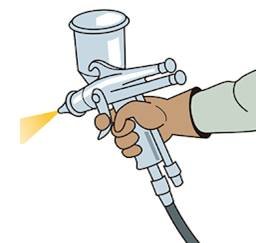
Inks
Ink is a gel or a solution which contains a dye or a pigment and is used to produce an image, text or a design. Ink is a complex medium composed of solvents, pigments, resins, lubricants, solubilizers and other additives. The pigment or the dye give the ink its colour. It is this pigment which determines the properties of the printed patterns. In Inks and sensors lab, we replace the pigments of an ink with conductive micro and nano materials such as Silver, Carbon, Graphite etc. to produce conductive ink. The major applications of these conductive inks are in the field of flexible electronics and printed sensors. As part of the ongoing activities of our lab, we use our custom-made conductive inks in printing sensors. The sensors thus printed on flexible substrates such as polymer sheets, paper or cloth, become flexible printed sensors. Flexible sensors find varied applications in wearable devices, smart clothing, tattoo sensors etc
Conductive Ink
Conductive ink is an ink that results in a printed object that conducts electricity. It is typically created by infusing conductive materials into a binder medium which satisfies printing ink properties. Conductive ink has a variety of applications in photovoltaics, touch screen edge electrodes, automotive, in-mound electronics, electronic textile and wearables, 3D antennas, conformal printing, EMI shielding, 3D printed electronics, ITO replacement (hybrid, direct printing), printed piezo resistive, capacitive and bio sensors, PCB (DIY/hobbyist, professional), RFID (HF, UHF), printed TFT and memory, OLED and large-area LED lighting, flexible e-readers, reflective displays, large-area heaters (battery, plant, seat, etc.) and more. Efforts are underway to develop the means to produce such inks at affordable cost.

Printed Sensors
Printed sensors are the primary building blocks for developing the Internet of Things and creating smart products and objects. They enable monitoring of physical parameters from temperature and moisture to pressure and motion.
Traditional sensors use rigid materials such as silicon, ceramics, and glass and are bulky, fragile, and expensive to produce. Printed sensors are made with polymers and specialty inks that are placed directly onto a substrate such as plastic, foil, paper, or textile. They offer a number of benefits, including:
- Creating smaller, more flexible products
- Cost-efficient mass production
- Reducing material cost by integrating sensors with other components
- Sensor capabilities over large areas
- Fast responses to stimuli
- Ideal for flexible displays, batteries, and solar products
Printed Electroencephalogram (EEG) sensors
Electroencephalography (EEG) is a method to record an electrogram of the electrical activity on the scalp that has been shown to represent the macroscopic activity of the surface layer of the brain underneath. EEG sensor system is a network of sensors which are attached to the scalp using a conductive gel. The printed sensors uses nanotechnology solutions to eliminate the usage of the conductive gel and makes it a simpler and user friendly sensor system.

Printed Electroencephalogram (EEG) sensors
Wearable EMG Strips
Electromyography (EMG) is a diagnostic tool primarily used for assessing the electrical activity of the muscles. The proposed EMG device would be a wearable system, conformable to any surface of the human body. Primary application is continuous monitoring of the muscles’ activity, which is required in the sports industry. The product also finds applications as a functional monitoring system for prosthetic arms, EMG-driven robotic arms for after-stroke rehabilitation, and can be used in nerve conduction studies. EMG also has niche applications as a discriminating tool to differentiate true labor pains from the other false alarms.
EMG System

The system has two parts:
- Disposable sensor surface which can be easily plugged to
- Reusable electronics along with IOT based EMG wave generator application.
Sensing Surface: Screen printed electrodes, SENIAM standards
Electronics: Electronics is designed on a flexible PCB, capable of signal acquisition and transmission. Signals are received and displayed on a mobile screen wirelessly using Wi-Fi. The entire system sits conformal on the skin surface inside a housing which can be pasted on the skin using medical grade adhesives.
Nanosensor for Rapid Detection of Staphylococcus aureus Human Pathogen
Staphylococcus aureus is a major human pathogen which causes a wide range of infections in human beings. Detection and identification of this pathogen is crucial for proper management of patients. Although a variety of testing methods are available for the detection of this pathogen, they are time consuming and their performances vary from setting to setting and need improvement. Rapid detection of this pathogen is the need of the hour. To cater to this need, the team has developed a low cost, nanomaterial based sensors for rapid detection of S. aureus pathogen.

The developed sensor has shown good sensitivity towards various concentrations of the said pathogen under laboratory conditions. The sensor shows high selectivity towards S. aureus against other human pathogens.
Nanomaterial based coatings:
With the development of functional nanomaterials, nanomaterial-based coatings are now becoming smarter, stronger and more durable. Nanocoatings, apart from serving as a physical barrier or decoration for the coated surface, also act as a multifunctional and smart interface. The barrier and mechanical properties of the organic coatings get enhanced by embedding nanofillers into them. With the incorporation of composite nanomaterials, smart coatings are being researched at the lab. They include self-cleaning coatings, anticorrosive coatings, heat-resistant coatings, anti-scratch coatings, hydrophobic and oil repellent coatings.
Gold-on-plastic Electrode-based Biosensors:
Gold-on-plastic is a new name given to materials recovered form e-waste. These materials have a thin nanolayer of gold on a plastic substrate. Samples are cut out of this material to be used as electrodes for the development of sensors. Such electrodes are very cost effective as they undergo a quick process of recovery form waste. Nanomaterial based glucose biosensors were developed on such electrodes and tested for its sensitivity and selectivity, and were found to be a low-cost alternative for the commercially available glucometer strips.
In-mold electronics (IME)
In-mold electronics is an advanced technology that combines the in-mold decorating process with printing of conductive inks. It is a process of integrating printed decorations and electronic circuitry with thermoforming and molding. The capacity to print electronic circuitry on a 2D substrate prior to converting it into a functional 3D part represents many manufacturing and material challenges and innovation/development opportunities.
- Titanium dioxide based bioelectric sensor for the acquisition of Electrocardiogram signals, Uma Ullas Pradhan, Narendra Reddy, Chandrashekar K and Mohan C. B., Microchemical Journal – Elsevier, 160, 2021, 105656. IF: 4.821
- Rapid Detection of Staphylococcus aureus Using Graphene Oxide Coated Screen-Printed Sensor Strips, Uma Ullas Pradhan, Vasudha Chandrashekar and Nanganand G S, Journal of Scientific & Industrial Research, Vol 79, 2020, 340-343. IF: 1.056
- Green Energy from Discarded Wool and Fish Scales, Prajwal Battampara, Deepak Ingle, Vijaykumar Guna, Uma Ullas Pradhan, Narendra Reddy Waste and Biomass Valorization,(2021) 12:6835-6845, Springernature.com, IF: 3.703
- Multiwalled Carbon Nanotubes enhance the Response and Sensitivity of the Ammonium Biosensor based on Alanine dehydrogenase. UshmabenChandrakantbhai Dave, Deepak Ingale, KrishnaVenkatesh, Venkata Krishna Bayineni, and Ravi-Kumar Kadeppagari. Journal of Electroanalytical Chemistry. (2017) 784:102-108. IF: 3.012
- Epi-Fluorescence Microscope
- Milli-Q Model DQ3 System
- Freeze Dryer Gamma 2-16 LSC Plus
- CRO
- Signal Generators
- Semiautomatic Screen-printing machine
- Triple Roll mill
- Industry grade Emulsifier
- Industry grade Centrifuge
- Study and fabrication of an Aptamer based FET biosensor – DST
- Exploring the Dynamics of Pancreatic Peptide-Membrane Interactions through Nano-scale Imaging: Implications on Type II Diabetes Mellitus – SERB-DST
- Design and Development of an Electrochemical Immunosensor for the Detection of Amyloid Beta in Biological Fluids of Alzheimer’s Patients collected on Dried Matrix Spots – BIRAC-CEFIPRA
- Antioxidation Coating for high temperature applications – AGI
- Nanomaterial based oil repellent coating for makeup brushes – Indeutsch
- Development of an Electrochemical Biosensor System for the Rapid Detection of Biowarfare Agents – DRDO
- Development of High Strength 3D-Chitosan Based Products for Biomedical Implants – DIC
- Development of a Novel Hemostatic Material as a Rapid First Aid Solution – BIRAC-SRISTI
- Development of Affordable IoT Based Soil Health Monitoring System for the Increased Crop Production – SSPS

Chandrasekhar K
Chandrasekhar K, Professor at the Centre, obtained his Ph.D. from VTU and researches in the domain of signal processing & communication. He has contributed in building various new knowledge base to the domain on subjects like auto-correlation matrix implementation in LabVIEW™, and Monte Carlo simulation and its importance in data analysis using LabVIEW™. In his previous assignment he headed the M.Tech.program in DSP & RF Communication streams at the Centre for Emerging Technologies. Prior to that, he was Head of the Department of Telecommunication Engineering at KSIT, Bangalore, and was instrumental in building up the department, and the facilities, ground up. He has been in the academic field for 28 years. He is a Reviewer for the International Journal of Communication Systems.He was an invited session chair for national conference and is a member of the LIC committee, VTU. He is a life member of ISTE, FIE, and IEEE .He has many publications in journals and has presented at various conferences and workshops. His extracurricular activities include table tennis, cricket, football and swimming.
chandra.k@ciirc.jyothyit.ac.in

Uma Ullas
Uma Ullas holds a Ph.D. in Electronics from the University of Mysore. She is currently an Associate Professor at the Centre, Earlier, she was a courtesy Associate Professor at the Department of Electrical and Computer Engineering at Florida International University, Miami, USA, between January 2017 and February 2018. She has over 23 years of academic, research and consultancy experience. Her core areas of work include nanomaterials-based coatings, nanomaterial-based sensors, nanomaterial-based conductive inks, with special interest in biomedical devices.
Uma is actively engaged with industry for various nanomaterial-based activities. She is a research consultant for Indeutsch Industries Pvt. Ltd., AGI resources Ltd., SJS Enterprises Pvt. Ltd. She has published several papers and has written book chapters in international and national journals. She is a member of the Board of Studies and the Board of Examiners of various institutions. She has also authored a book on electronics for students pursuing Bachelor’s degree at Bangalore University.
Email id : uma.ullas@ciirc.jyothyit.ac.in

Deepak Ingale
Deepak Ingale has a Master’s in VLSI and Embedded Systems. He has over 12 years of academic experience and two years of industrial experience with Wipro Technologies. He has worked as an Assistant Professor at the Centre for Emerging Technologies and had been involved in setting up a DSP Laboratory, where he actively taught M.Tech.students. He has designed and delivered value added programs on PCB Designing using KiCad, LABVIEW and built embedded systems for hobby using ARDUINO.
He was involved in designing the electronics part of the nano-biosensor for ammonia detection and used in micro air vehicles for a project funded by NP-MICAV (DST-DRDO). He is a mentor for Atal Tinkering labs,student innovator program, under Atal Innovation Mission, where he guides and helps students from various schools across the country to take their innovative ideas to the prototype stage, and finally to product level. He and his team also provide consultancy services to start-up companies by implementing hardware and software solutions for IoT platforms and also helps them in resolving technical issues. He has published several papers in various national and international journals and is working as an Assistant Professor at the Centre.
Email Id: deepak.vi@ciirc.jyothyit.ac.in

Keshava Gowtham
Keshava Gowtham, currently working as a Research Engineer, B.E. in Information Science and M.Tech.in Computer Networks from VTU, and has an overall work experience of about eight years. He has worked on Micro Air vehicles Systems peripheral interfacing, comprising of various MEMS sensors and ARM-based microcontrollers. His areas of interest includes embedded devices programming, IoT and Android app development. He has extensively worked on developing the prototype for the juvenile arthritis machine developed in the lab and completed a number of IoT related in-house projects. He is a mentor for Atal Tinkering labs, a student innovator program under Attal Innovation Mission, where he has guided and helped students from various schools across the country to take their innovative ideas to the prototype stage, and finally to product level.He and his team also provide consultancy services to start- up companies by implementing hardware and software solutions for IoT platforms and also helps them in resolving technical issues.
Email Id: keshava.gns@ciirc.jyothyit.ac.in

Kashma
Kashma is currently working as a research scientist, developing biosensors for resource-limited settings. She has been awarded a fellowship from the Department of Science and Technology under the women scientist scheme to support her work on pathogen detection using biosensors. She has entrepreneurial experience, being part of a start-up and has attended numerous workshops including a bootcamp conducted by IIMB. Her core background is in Electrical Engineering with a Ph.D. specializing in Electro-Optics from Drexel University, USA. Her dissertation work focused on designing and fabricating thin films, for remote sensing applications. This was a NASA funded project and resulted in a patent. Her multidisciplinary background includes electrical engineering, optics, material science and biotechnology.
Email Id: kashma.rai@ciirc.jyothyit.ac.in