Overview
The surface of a material is the host to a number of activities, including chemical, optical, electrical, electronic and magnetic interactions. This is because, atoms on the surface encounter a different environment than that of their bulk counterparts. Atoms inside the bulk of a material are surrounded by similar/identical geometric configurations; on the other hand, atoms on the surface, are attached to the material on one side by either chemical/physical bonding, the other side is free. The absence of neighbouring atoms on one side results in an imbalance in the force experienced by the surface atoms. In such a scenario, the surface atoms try to find an equilibrium structure which is different from that of bulk. This could happen in two ways: relaxation and reconstruction.
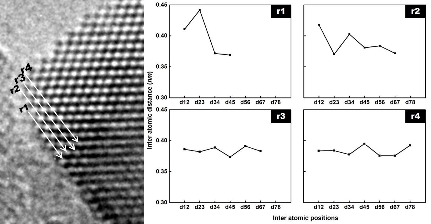
Demonstration of Surface Reconstruction: Magnified portion of the ceria particle and the corresponding inter atomic distance plots of four outermost atomic rows along {100} facet. (Appied Physics A, 128(1), 1, 2022)
Normally in metals, in-plane atoms on the surface try to increase their inter atomic distance and interlayer spacing (relaxation). These changes decrease and tend towards standard bulk values as one move deeper inside the materials (bulk). But, in some materials, normally in semiconductors, atoms on the surface assume entirely different structure from that of the bulk, to compensate for the absence of neighboring atoms. This is called reconstruction.
In essence, there is a lot of activity happening on the surface, and if one can increase the number of atoms on the surface compared to bulk, activity of a material increases manifold leading to drastic changes in chemical, thermal, electrical and many other physical properties of a material. This is what exactly happens in nanomaterials.
Changes in properties can largely be attributed to change in surface-to-volume ratio as more and more number of atoms occupy the surface, and, more often than not, this and the resulting quantum size effects makes these nanoparticles more active to its surrounding environment. Most of the recent research is to modify and tune these properties so that it could be useful to mankind via medical, energy related and catalytic applications to name a few.
Another scenario is when the surface of material is attached to another material. The resulting interface also throws up a lot of interesting physical phenomena wherein, atom on one surface tries to bond with a different atom leading to interface relaxation, epitaxial growth and even formation of defects. So, fundamentally, surfaces and interfaces of materials are one of the most exciting areas of physics. A detailed structural and chemical study of such surfaces/interfaces would help in understanding a host of material properties which are important in energy, environment related applications.

Three of the major areas being looked upon in this lab are multilayer thin films for energy applications, embedded nanostructures in insulating matrices for opto-electronic applications, and tuning nanoparticle orientations to increase their surface activities.
Study of oriented multilayer thin films on crystalline substrates: When a system comprises of surfaces and interfaces, there are lot of potential activities happening at the interfaces as well on the surface (as explained in the figure below). In such cases orientation of the substrate plays a very important role.

For example, when gold thin film is deposited on a Si(110) substrate, the gold-silicon interface tries to arrive at a minimum energy configuration which influences the final morphology of the thin film itself. Moreover, if the system is subjected to higher energy (heating), interface mixing takes place, leading to drastic changes in surface morphology which is hugely influenced by the orientation of the substrate. Studying such interfaces involving Semiconductor/Metal Oxide/Metal thin films is one of the projects being undertaken in this lab. Here, selected metal oxide thinfilms is being deposited using various Physical Vapour Deposition techniques (including Thermal, Pulsed Laser and Magnetron sputtering deposition) and then analyze whether orientation of the deposited thinfilm has any effect on its electrical, optical, chemical and structural properties compared to randomly deposited thin films, right down to nano/atomic level.
Embedded nanostructures: Light absorption/conversion efficiency of semiconductor nanostructures mainly depend on five major criteria. First and the most obvious one will be size of the nanoclusters. Apart from that, embedding matrix, amorphous/crystalline nature of the nanostructures, presence of surface and interface states, shape of the nanostructures also have substantial effect on light absorption property. Si and Ge quantum dots (QD) are the major elemental species being explored; especially Ge QDs have received renewed interest in recent times because of larger bulk absorptioncoefficient, larger exciton Bohr radius, which makes band gap tuning easier, and lower synthesis temperature among others. In this project,the objective is to study the matrix-QD interface, effect of inter QD distance and process of agglomeration of Ge ions into Ge nanocrystallites at high temperatures in-situ. Low energy elemental ions will be implanted in dielectric matrices. Process of incident ions agglomerating into amorphous/crystalline nanostructures and then the structural and chemical properties of Ge/SiO2 and Ge/Si3N4 interface shall be studied in detail.
Oriented Nanocrystals: Apart from reducing the size of a material to increase number of surface atoms, crystalline orientation of a nanostructure also plays an important role in defining its physical properties. It is well known that the surface activity of a nanocrystal essentially involves interaction of surface atoms with surroundings. The ease with which, making and breaking of chemical bonds that take place between the surface atoms and the surrounding environment depends on surface crystalline orientation. This is because, number of reactive sites on the surface (ex: dangling bonds) varies with crystalline orientation. So, apart from reducing the size of the nanoparticles, the morphology of nanoparticles can be tuned. This leads to the exposure of the most active surfaces. The main aims of this project are in identifying specific metal-oxide systems and tune their shapes to increase their surface activity and thereby catalytic efficiency.
Endotaxial nanostructures by low energy ion implantation:
Coherently embedded metal nanostructures (endotaxial) are known to have potential applications concerning to the areas of plasmonics, optoelectronics and thermoelectronics. Incorporating appropriate concentrations of metal atoms into crystalline silicon is critical for these applications. So, choosing proper dose of low energy ions, instead of a depositing thin film as a source of metal atoms, helps in avoiding surplus concentration of metal atoms that diffuses into the silicon crystal.In this work, 30 keV silver negative ions are implanted into a SiOx/Si(100) at two different fluences. Embedded silver nanostructures have been characterized by using planar and cross-sectional TEM (XTEM) analysis.

Planar and XTEM micrographs of silver endotaxialnanostrcutures (Applied Physics A, 124(6), 402, 2018)
- Role of oriented ceria nanoparticles in the decomposition of carbonized sucrose. SK Gundanna, A Mitra, KGL Bhatta, and UM Bhatta. Applied Physics A:Materials Science and Processing,218 (2022). IF: 2.5
- Effect of thermal treatment on the surface/interfacial behaviour of Au@ SiO2 nanoparticles in the presence of CTAB surfactant molecules. SK Gundanna, A Mitra, KGL Bhatta, and UM Bhatta. Powder Technology, 381 (2021), 503. IF: 5.13
- Effect of thermal annealing on structural and electrical properties of TiO2 thin films. RM Nagabharana, GN Kumaraswamy, SK Gundanna, and UM Bhatta.Thin Solid Films710 (2020), 138262 IF: 2.18.
- Growth of embedded Ge nanoclusters inside spatially confined SiO2 matrix: An in-situ TEM study. SK Gundanna, P Guha, N Kiran, and UM Bhatta,Physica E: Low-dimensional Systems and Nanostructures, 114 (2019) 113637. IF: 3.38
- Structural characterization of magnetron sputtered ZnO thin films on Si(100) using RBS, scanning and high resolution transmission electron microscopy methods. RM Nagabharana, N Kiran, P Guha, and UM Bhatta. Surfaces and Interfaces, 15 (2019) 239 IF: 4.83.
- Low speed Diamond Saw
- Automated Polishing Machine
- Muffle Furnace
- Tubular Furnace
- Customized IV measurement system
- Structural and chemical properties of interfaces of Si/glass-based metal/metal oxide thin films for solar cell applications. SERB, DST.
- In-situ TEM study of nucleation and growth of embedded Ge nanostructures in SiO2 and Si3N4 matrices. UGC-DAE-CSR

Umananda Bhatta
Umananda M Bhatta obtained his Master’s from University of Mysore, followed by Ph.D. in Physics from Institute of Physics (IOP), Bhubaneswar, affiliated to HomiBhabha National Institute (DAE undertaking). During his Ph.D., he was instrumental in developing in-situ TEM facility at IOP, where he conducted an extensive study on temperature dependent behaviour of Au thin films on various Si substrates. After completing his PhD, he was selected to work on an Engineering and Physical Sciences Research Council (EPSRC), UK, project, and undertook his postdoctoral research at the department of materials and engineering, University of Sheffield. During this time, he worked on a project titled, “Building Ceramic Metamaterials from Nanoparticles: A combined Modelling, Tomography and In-situ Loading Study”, as part of an EPSRC project which involved collaborations with several other distinguished universities from thaUK and USA. During his postdoctoral stint, Bhatta played a key role in studying the surface properties of ceramic nanomaterials using advanced electron microscopy techniques, including aberration corrected microscopy, nanotomograpy, electron energy loss spectroscopy (EELS) and nanoindentation, among others.
His major specialization includes advanced electron microscopy and associated techniques. He has vast experience in other domains of experimental surface physics, including X ray diffraction, X-ray photoelectron spectroscopy, ion beam synthesis and characterization. His main research interests include interactions at surfaces/interfaces of different nanomaterials/hetero epitaxial thin films, ion beam synthesis (IBA), and characterization and in-situ thermal and mechanical studies of nanomaterials.
He received the DST Young Scientist Research Grant through which he worked on a project titled, “Structural and Chemical Studies of metal/metal oxide thin films on glass/silicon surfaces for solar cell applications”. He is also involved in a collaborative project with UGC-DAE-CSR in the field of Ion Beam Synthesis of embedded nanostructures.Currently, he is an Associate Professor at CIIRC.
GoogleScholar: http://scholar.google.co.uk/citations?hl=en&user=vcuI5skAAAAJ&view_op=list_works&cstart=20
Email Id: umananda.b@ciirc.jyothyit.ac.in

Susheel Kumar G
Susheel Kumar G obtained his M.Sc. in Physics from Bangalore University and joined Surface and Interface group at CIIRC in 2018 as a Research Assistant. He has experience of using sophisticated instruments such as SEM, XRD, TGA, UV-Vis Spectroscopy, FTIR, etc. His main research areas include synthesis of embedded nanostructures using low energy ion implantation and chemical methods, electron microscopy of nanostructured materials, and surface/interface characterization.